8-bit Computer
Initial Build Review
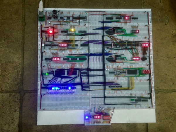
The initial build of my 8-bit computer is complete. It’s mostly as designed by Ben Eater, except where components weren’t easily available or where I already had usable alternatives. Youtube will yield plenty of examples of people running Fibonacci or counting from 0 to 255 and back again so I won’t waste time on a video at this stage. Instead, here’s a photo of it powered-up:
Review
Overall, it’s a great project to build and I recommend it to anyone geeky enough to be interested in this sort of thing. It’s improved my knowledge of how computers work and sparked a whole load of really enjoyable dives down the rabbit hole. Of course, it’s not perfect (what is?). My biggest issue has been nothing to do with Ben’s design and everything to do with the cheap breadboards I used. Beyond that, it was designed as a very simple educational project rather than anything more advanced so has the potential to quickly become little more than a large and rather expensive dust-attracting device after you’ve built it and programmed it with a few simple numeric routines. This is fine if you want a fun little project and will reuse the parts, or if you want to get some hands-on lessons on basic CPU operation. However, if you use it as a springboard to explore the wider topic of CPU architecture then it really will open a whole world of possibilities. What follows are some details of what I see as the original design’s shortcomings and the improvements I have planned:
Memory address space:
The memory address space is currently 4 bits, giving a whole 16 bytes of program and data memory. It currently has a 2Kx8-bit RAM chip and it’d be good to make more of this available.
Program Counter:
The program counter is also 4 bits. If I’m going to make room for larger programs, this will also need to be increased.
Program Loading:
Loading programs into RAM is done manually … with itty-bitty switches … every time you turn the computer on. While this is just about tolerable for 16-byte programs, it’s going to get very tedious, very quickly, when I increase the memory. I’ve considered various solutions to this and settled on using EEPROM and a USB-to-serial link so I can upload programs directly from my computer and retain them over power cycles. I’ll probably design it with switchable 256-byte banks on the EEPROM to allow for multiple programs to be stored and to avoid exceeding 8-bits for the addressable space. This will mean I have separate program and data memory (see below for more on this).
Arithmetic Logic Unit (ALU):
This is probably my least-favourite part of the computer so far. I’ve had a lot of trouble getting the ALU to work reliably due to the amount of wiring and the crappy breadboards. With only add and subtract functionality, it’s also quite limiting. The 7400-series actually has a full-featured ALU (74xx181) so I should be able resolve both of these issues with two of those.
Instruction Set:
If I’m going to upgrade the ALU then I’m going to need to make room for more instructions. The current design allows for a maximum of 16 instructions and the ALU I plan to use has that many different modes so there will be no room for anything else. The way instructions are written in program memory is also going to have to change to accommodate the increased memory address space.
Control Module:
The 2K x 8-bit EEPROMs used to store the instructions have 11 address lines, of which the current design uses: 4 for the instruction, 3 for the step counter, 2 for the flags and 1 for the bank select. That isn’t enough if I want to add more instructions, status flags or control lines. Did I mention that the control module is my second least-favourite part of the computer? The whole thing is going to need a bit of a rethink but don’t worry, I have a cunning plan.
Output:
Outputting data to a 4-digit, 7-segment LED array is fine but it would be much more fun if I could control actual hardware or send output to some kind of display screen. I haven’t decided exactly what I’m going to do yet but the architecture should provide for multiple, addressable output devices.
Input:
Some kind of input would be nice. At the least, an 8-bit DIP switch and some kind of simple routine which waits for user input. I may make a keyboard or an ADC if I get carried away.
Size:
Another factor in the utility of the computer is its size. 14 breadboards take up a lot of space and they don’t make for very reliable wiring if you’re poking about with things (especially if you bought crap ones like I did). I want to be able to use it on my lap comfortably so I plan on reducing the number of breadboards as much as possible during development. I’ll achieve this by committing unchanged modules (A & B registers, output module, clock) to protoboard first and then the others as I complete them. My idea is to retain the modular approach so I can reconfigure the computer and experiment with different designs without needing a full rebuild every time.
Conclusion
The computer, as designed, uses the Von-Neumann architecture where program and data memory share the same space and everything moves around on the same bus. Ironically, my thinking around solving the issues described above led me to reinvent the Harvard architecture, or something close to it (did I mention this has been a fascinating and educational project?). Once I discovered the existence of the Harvard architecture and learned more about it, a few other ideas dropped into place and the shape of an improved computer started to come into focus.
Future posts on this topic will document the planned changes so follow along if you’re interested.
Posted on 19 February 2019